Quality
CNAS Nationally Accredited Laboratory

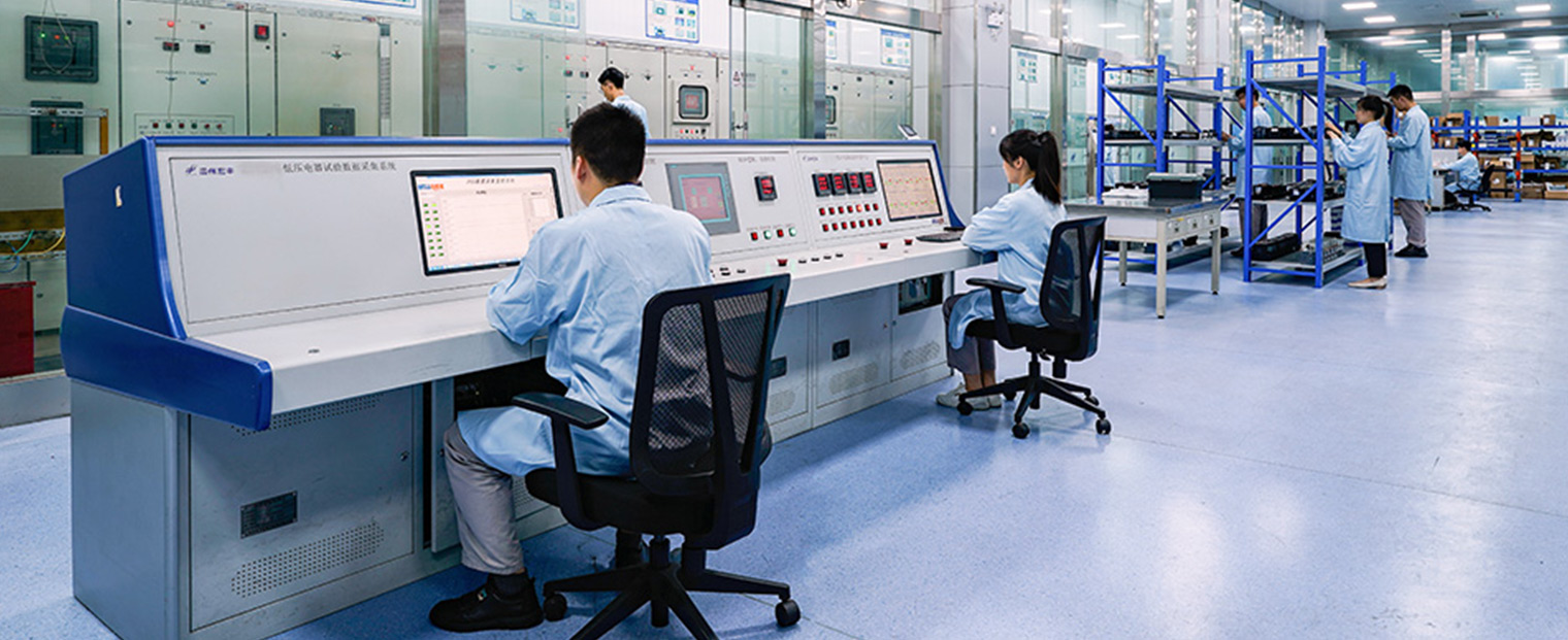
The CNAS nationally accredited laboratory was developed from the testing center founded in 1997 and expanded in 2012. In 2014, it obtained an Accreditation Certificate in accordance with ISO/IEC 17025 issued by the China National Accreditation Service for Conformity Assessment.

The company's CNAS national accredited laboratory is a material testing base with perfect testing facilities among the domestic counterparts, which provides one-stop testing and experimental solutions for the company's material research and development, product quality control, material application research and product failure analysis. At present, it has formed a complete set of material testing and testing system, such as metrological calibration, chemical composition analysis, organizational structure analysis, physical and mechanical properties testing and electrical properties testing. At the same time, the laboratory is equipped with professional technical and managerial personnel in various specialized fields, as well as advanced analytical test instruments and equipment in the industry.

Since its establishment, the CNAS nationally accredited laboratory of Hongfeng has made significant improvements in both testing management and testing capabilities. The laboratory now has a complete and effective quality management system and is renowned for its standardized operation, excellent technologies, and high-quality services.

Field Emission Scanning Electron Microscope

The Zeiss GeminiSEM 300 can perform Inlens secondary electron imaging and backscattered electron imaging simultaneously with a resolution of up to 0.7nm. It can realize fast, high-quality, distortion-free large-scale and sub-nano resolution imaging. The EDS detector with a 100 mm2 window can perform real-time quantitative determination of point, line, and area elements. The EBSD detector can collect distortion-free and megapixel-resolution EBSPs for detailed strain and phase analysis.

ICP-OES

The Spectro Arcos ICP-OES has a vertical double observation structure (DSOI) that increases sensitivity and eliminates contamination/matrix compatibility issues. Its ORCA optical system can capture spectra in the 130-770 nm range. Compared to Echelle-based systems with cross-dispersion using a middle step grating and prism, it delivers performance in the UV/VUV range with photoacoustic signal intensity ranging up to 5x more.

OES

The SPECTROLAB S features the world’s CMOS-based detector recording system, making it ideal for high-end metal analysis. It provides extremely fast, highly accurate, and exceptionally flexible analysis for applications ranging from trace elements to multi-matrix.

Atomic Absorption Spectrometer

The Jena novAA 800F features an integrated carousel with an RFID reader for 8 coded hollow cathode lamps, deuterium background correction, a proven optical bench in single and double beam mode as well as in emission mode, and the latest SiOSens solid-state detector. Its multiple intelligent accessories maximize productivity, safety, and ease of use for analytical routines.

Universal Material Testing System

The 68TM-30 universal material testing system has 30kN and 1kN load sensors with an accuracy of 0.5 grade in the range of 0.1 ~ 100%. The test system can perform integrated data closed-loop control and acquisition, as well as automatic identification and calibration of sensors. Its high-precision non-contacting video extensometer AVE2 has a resolution of 0.5μm and uses a patented cross-polarized lighting system and CDAT fans to eliminate the influence of personnel, lighting, and airflow on the test results for highly repeatable and accurate strain measurement.

3D Project

The VR-5200 project uses striped structured light and a high-precision CMOS sensor to capture images and measure the height and position of each point. Equipped with a low-power lens, it can measure ranges up to 200×100×50 mm. The high-magnification lens reduces the display resolution to 0.1μm, allowing for non-contact batch measurement of shape, fluctuation, and roughness. 

Image Dimension Measurement System

The IM-8020 uses a dual telecentric lens with exceptional edge detection capabilities to measure samples of varying heights with just one click. Its detection performance is 3 times that of conventional models thanks to its 20-megapixel CMOS and new edge detection algorithm. With a measurement area of 300 mm × 200 mm and twice the speed of traditional models, it can measure up to 300 parts in just a few seconds. This allows for fast, accurate, and easy measurements, greatly improving accuracy while reducing measurement time and human error.

Laser Particle Analyzer

The HELOS/BR laser particle analyzer is equipped with a powerful and robust RODOS dry dispersion unit for fast and repeatable particle size analysis of dry samples. It has a measuring range of 0.3 to 175μm and an accuracy of less than 0.3%.

Simultaneous Thermal Analyzer

The STA 449F3 Jupiter is a robust, flexible and easy-to-use instrument that simultaneously determines calorie effects and mass variation. It combines a high-performance Heat-Flux DSC with a thermobalance that has microgram-resolution, offering an unmatched sample load and measurement range.

Low-voltage Electrical Appliance Test Station

The low-voltage electrical appliance test station of Hongfeng was established in 2013. The actual application scenario of a material is simulated to study its application characteristics, and preliminary tests are conducted for new projects to predict the product applicability of new materials.
After years of progress, the test station has acquired comprehensive low-voltage electrical testing capabilities and is now capable of testing the electrical life, temperature rise, short circuit, and other items of contactors, circuit breakers, relays, protectors, etc.

Wenzhou Hongfeng Electrical Alloy Co., Ltd.